Beam Pen Lithography (BPL) - Desktop Nanoprinting Enabled by Compact 3D Nanopositioning Stage
Desktop nanoprinter based on a novel, highly scalable, and versatile photolithographic technology and XYZ piezo-driven nano-precision stage finds applications in photonics, meta-materials, electronics, soft robotics, and biomedicine.

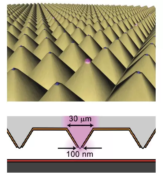
Nanoscale components have applications in semiconductor manufacturing, medical technology, and photonics. Lithography is one way to produce miniscule structures. However, just like with classical microscopy, the resolution of optical lithography suffers from the diffraction limit. Over the past few decades, near-field and super-resolution techniques have aided modern microscopy to overcome this limit and related solutions were applied in lithography. However, achieving high resolution and high throughput with one single technique has been difficult. Recent lithography advances based upon scanning probe microscopy and arrays of transparent pyramid-shaped elastomeric tips, now allow patterning of molecules over large-areas with high-throughput.
Millimeter-Scale Nanostructured Patterns, Diffraction-unlimited Resolution
A new parallel technique, called beam pen lithography, can toggle between near- and far-field distances, allowing arbitrary patterns of both large and sub-diffraction limit features to be generated by passing light of a desired wavelength through nanoscopic apertures at each tip in the array.
One of the advantages of BPL is its flexibility to create arbitrary, programmable patterns, independent of fixed photomasks with no need to create a new master for each variation. This maskless technique saves both time and cost, making it ideal for prototyping.
Piezoelectric XYZ Nano-Precision Stage Provides Motion in 3-DOF
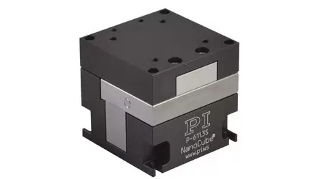
Highly accurate motion in X, Y, and Z is needed to make BPL work. The motion part is handled by a closed-loop P-611 piezo flexure stage. This nanopositioning system precisely moves the substrate under the beam pen array between light exposures and enables rapid reconstruction of an arbitrary, high-resolution pattern - up to 100,000s of sub-250 nm pixels at a time. The nanopositioning stage is actuated by special multilayer piezo stacks whose ceramic encapsulation provides protection against humidity and moisture, important in bio-chemical applications.
Novel Applications
The ability to rapidly prototype and fabricate millimeter-scale nanostructured patterns and devices with sub-diffraction resolution not only reduces the time and accelerates the discovery, but it also enables routine fabrication of structures and devices not previously possible.


- Bioprinting and Tissue Engineering
Bioprinting is one of the many applications of the TERA-Fab™ E series platform. It allows the production of tissues for reconstitution and organs for transplantation. Even the food industry, a massive economic sector that benefits greatly from genomic engineering, is showing interest in this emerging field. The possibility to bring down the cost for rapid fabrication of more accurate, i.e. more biologically relevant bioconstructs for tissue engineering and pharmaceutical applications, has the potential to transform industries.
- Applications in Confined Chemical Synthesis and Highly Localized Photochemistry
BPL enables the synthesis of structures with nanoscale resolution and can generate millions of attoliter-sized nano-wells that serve as “nanoreactors”. The TERA-Fab™ E system is useful for biochemical applications because of its ability to immobilize and photochemically synthesize/modify many types of biological structures with feature sizes that are similar to those found in biological and living systems.
- Applications in Electronics
Complex structures used in electronic circuits can also be produced with the maskless tool. To provide an example for the addressable dimensions: fully functional resistors, capacitors or inductors of several millimeter length by a few micrometer width and comprised of an array of nanowires (<200nm) have been produced.
Why NanoCube?
Says Andrey Ivankin, CTO and Co-Founder of TERA-print, “TERA-print set out to develop desktop nanoprinters that offer high, in some cases sub-100 nm, resolution patterning of a wide range of materials. This demanded a piezo stage that allows for precise motion in XYZ, is compatible with high relative humidity environments to conform with a wider range of molecular inks, and can also tolerate the force generated by 100,000s of beam pens brought into contact with the substrate. NanoCube from PI met all of these requirements in an extremely compact format with the added benefit of German engineering quality and reliability.”
More information about the TERA-print and its Desktop Nanoprinter is available here: https://www.tera-print.com/

